Clamp check
When a flyback’s switch turns off, the magnetizing current passes to the secondary. The current in the leakage inductance cannot: it drives the drain above the input voltage plus the reflected output voltage until a clamp across the primary conducts [Kollman 2024]. The clamp check takes the worst-case operating point and the clamp’s data, all in SI units. It shows:
- the reflected voltage, the leakage energy and the time the leakage current takes to fall to zero;
- the clamp voltage at the actual peak current, and the switch voltage against its rating;
- the clamp dissipation;
- with a TVS, the output voltage the flyback runs up to without a load.
Each result names its equation. The chart shows how the dissipation and the switch voltage trade against the clamp voltage.
What it computes
Section titled “What it computes”Enter the largest input voltage and the largest peak primary current at turn-off. If they occur at different operating points, checking them together is conservative. The turns ratio is 1:, where is the secondary turns divided by the primary turns, and is the leakage inductance referred to the primary.
Reflected voltage
Section titled “Reflected voltage”While the output diode conducts, the primary winding carries the output voltage plus the diode drop, divided by [Erickson & Maksimović 2020, Ch. 6]:
- output voltage reflected to the primary
- output voltage
- output-diode forward drop
- turns ratio, secondary/primary
Assumptions, convention and source
- Assumptions
- ideal (lossless) switches and passive components
- output diode modelled as a constant forward drop V_D
- Notes
- the primary winding voltage while the output diode conducts; the switch then blocks plus this voltage
- Source
- Erickson & Maksimović 2020, Ch. 6 (Converter Circuits: the flyback's transformer model); derived here
- Derivation
- step-by-step sympy derivation
- Equation id
flyback.V_OR· equations.yaml entry
A clamp must hold a higher voltage than this. Otherwise it conducts whenever the output diode does, and takes the energy meant for the output.
Leakage energy
Section titled “Leakage energy”At turn-off the leakage inductance carries the peak primary current (leakage energy). The clamp takes that energy in every period (leakage power).
Clamp voltage
Section titled “Clamp voltage”A TVS starts to conduct at its breakdown voltage , and its voltage rises with its current. Its datasheet gives the clamping voltage at a peak pulse current . A dynamic resistance in series with the breakdown voltage models the rise between them [STMicroelectronics 2022]:
- TVS dynamic resistance
- TVS peak pulse current
- TVS breakdown voltage
- TVS clamping voltage at IPP
Assumptions, convention and source
- Assumptions
- TVS modelled by its breakdown voltage and a constant dynamic resistance
- Notes
- the resistance that, in series with the breakdown voltage, gives the datasheet's clamping voltage at its peak pulse current; it applies to the datasheet's pulse, since the dynamic resistance depends on the pulse duration
- Source
- STMicroelectronics 2022, clamping voltage = breakdown voltage + dynamic resistance x peak current, solved for the dynamic resistance at the datasheet's clamping voltage and peak pulse current
- Equation id
tvs.R_D· equations.yaml entry
The tool takes the TVS’s voltage at the peak primary current as the highest clamp voltage:
- clamp voltage
- peak current
- TVS dynamic resistance
- TVS breakdown voltage
Assumptions, convention and source
- Assumptions
- TVS modelled by its breakdown voltage and a constant dynamic resistance
- Notes
- a TVS clamps above its breakdown voltage: judge it by its clamping voltage at the actual peak current
- Source
- STMicroelectronics 2022, clamping voltage from the breakdown voltage and the dynamic resistance
- Equation id
tvs.V_clamp· equations.yaml entry
While the leakage current falls to zero, the TVS voltage falls back towards , so the tool shows the clamp voltage as a range.
An RCD clamp is a diode into a capacitor with a resistor across it. The capacitor holds the clamp voltage, and the resistor dissipates the clamp’s power. The clamp voltage settles where the two balance (the root above ; see the derivation linked under the equation):
- clamp voltage
- peak current
- leakage inductance (primary)
- clamp resistor
- output voltage reflected to the primary
- switching frequency
Assumptions, convention and source
- Assumptions
- the clamp holds a constant voltage while it conducts, so the leakage current falls linearly to zero
- RCD clamp: the capacitor's voltage ripple is small and its resistor dissipates the clamp energy
- periodic steady state
- Notes
- the resistor dissipates the clamp power, ; a larger resistor gives a higher clamp voltage and a lower dissipation
- Source
- Kollman 2024, RCD clamp: the trade-off between the clamp voltage and its losses; derived here
- Derivation
- step-by-step sympy derivation
- Equation id
clamp.rcd.V· equations.yaml entry
By this equation a larger resistor gives a higher clamp voltage, and by the dissipation equation below a lower dissipation: the clamp trades its voltage against its losses [Kollman 2024].
Switch voltage
Section titled “Switch voltage”While the clamp conducts, the switch blocks the input voltage plus the clamp voltage:
- switch voltage while off
- clamp voltage
- input voltage
Assumptions, convention and source
- Assumptions
- ideal (lossless) switches and passive components
- Notes
- after turn-off the leakage inductance drives the drain above until the clamp conducts and holds it at
- Source
- Kollman 2024, the leakage inductance drives the drain above the reflected output voltage; the clamp limits it
- Derivation
- step-by-step sympy derivation
- Equation id
clamp.Vds· equations.yaml entry
The margin is the switch’s rating minus this voltage, at the highest clamp voltage.
Reset time and clamp dissipation
Section titled “Reset time and clamp dissipation”While the clamp conducts, the magnetizing inductance holds the primary at . The leakage inductance therefore sees , and its current falls linearly to zero [Erickson & Maksimović 2020, Ch. 2]:
- time for the leakage current to reach zero
- peak current
- leakage inductance (primary)
- output voltage reflected to the primary
- clamp voltage
Assumptions, convention and source
- Assumptions
- the clamp holds a constant voltage while it conducts, so the leakage current falls linearly to zero
- Notes
- the leakage inductance sees while the clamp conducts; the closer the clamp voltage is to , the longer the reset, which must fit in the off-time
- Source
- Erickson & Maksimović 2020, Ch. 2 (Principles of Steady-State Converter Analysis); derived here
- Derivation
- step-by-step sympy derivation
- Equation id
clamp.t_reset· equations.yaml entry
The reset must fit in the off-time. The closer the clamp voltage is to , the longer it takes; the tool warns when it would take a whole switching period or more. The clamp would then conduct energy meant for the output, and the equations here no longer hold.
Meanwhile the reflected voltage keeps driving current into the clamp. So the clamp absorbs more than the leakage energy, and the closer the clamp voltage is to , the more it absorbs [Kollman 2024]:
- clamp loss
- peak current
- leakage inductance (primary)
- output voltage reflected to the primary
- clamp voltage
- switching frequency
Assumptions, convention and source
- Assumptions
- the clamp holds a constant voltage while it conducts, so the leakage current falls linearly to zero
- periodic steady state
- Notes
- the leakage energy per cycle times : while the leakage current falls, the reflected voltage keeps driving energy into the clamp, the more so the closer the clamp voltage is to
- Source
- Kollman 2024, clamp dissipation against the ratio of the clamp voltage to the reflected voltage; derived here
- Derivation
- step-by-step sympy derivation
- Equation id
clamp.P· equations.yaml entry
For a TVS, this equation at the highest clamp voltage is a lower bound, and at an upper bound. The table shows both, and their ratio to the leakage power.
Output voltage without a load
Section titled “Output voltage without a load”With the load removed and no regulation, the output keeps charging. It stops only when its reflected voltage reaches the clamp voltage, and from then on the clamp takes all of the input power. A TVS holds its voltage while it does, so the output stops at:
- output ceiling set by the clamp
- output-diode forward drop
- clamp voltage
- turns ratio, secondary/primary
Assumptions, convention and source
- Assumptions
- ideal (lossless) switches and passive components
- output diode modelled as a constant forward drop V_D
- fixed duty ratio, no regulation, load removed
- a clamp whose voltage does not depend on the power it absorbs (a TVS or Zener clamp)
- Notes
- without a load and without regulation the output charges until its reflected voltage reaches the clamp voltage; from then on the clamp takes all of the input power, which it must be rated for. An RCD clamp's voltage rises with that power (the resistor must dissipate it), so this bound does not hold for it
- Source
- Erickson & Maksimović 2020, Ch. 6 (Converter Circuits: the flyback's transformer model); derived here
- Derivation
- step-by-step sympy derivation
- Equation id
flyback.V_ceiling· equations.yaml entry
The output capacitor and everything on the output must withstand this voltage, and the TVS must be rated for the whole input power, far more than its dissipation in normal operation.
An RCD clamp gives no such bound. Its voltage is where its resistor dissipates the clamp’s power (the power balance behind the RCD equation above), so at no load, with the whole input power to dissipate, the clamp voltage rises far above its loaded value. The output and the switch voltage rise with it. The tool shows no ceiling for an RCD clamp and warns instead: limit the input power at no load, or add a fixed-voltage clamp.
Choosing the clamp voltage
Section titled “Choosing the clamp voltage”The chart plots the dissipation (logarithmic axis) and the switch voltage against the clamp voltage, from just above . A low clamp voltage costs dissipation, and a high one costs switch voltage. The switch’s rating sets the highest clamp voltage the switch allows. The shaded band is the range of the clamp entered.
Worked examples
Section titled “Worked examples”A TVS clamp:
| Symbol | Value | How it is obtained |
|---|---|---|
| input voltage | 72 V | given |
| output voltage | 12 V | given |
| output-diode forward drop | 500 mV | given |
| turns ratio, secondary/primary | 0.25 | given |
| leakage inductance (primary) | 2 µH | given |
| peak current | 2 A | given |
| switching frequency | 100 kHz | given |
| switch voltage rating | 150 V | given |
| TVS breakdown voltage | 60 V | given |
| TVS clamping voltage at IPP | 90 V | given |
| TVS peak pulse current | 10 A | given |
| output voltage reflected to the primary | 50 V | Flyback: output voltage reflected to the primary |
| leakage energy per turn-off | 4 µJ | Energy stored in the leakage inductance at turn-off |
| leakage energy times fs | 400 mW | Leakage-energy power |
| TVS dynamic resistance | 3 Ω | Dynamic resistance of a TVS from its datasheet |
| time for the leakage current to reach zero | 400 ns | Time the leakage current takes to fall to zero in a flyback's primary clamp |
| clamp voltage | 66 V | Clamping voltage of a TVS at a given current |
| switch voltage while off | 138 V | Flyback: switch voltage while the primary clamp conducts |
| clamp loss | 1.65 W | Power dissipated in a flyback's primary clamp |
| clamp loss | 2.4 W | Power dissipated in a flyback's primary clamp |
| output ceiling set by the clamp | 16 V | Flyback: open-load output voltage limited by the primary clamp |
With the peak current of 2 A, the TVS reaches 66 V, well below its datasheet clamping voltage at 10 A. The dissipation lies between 1.65 W and 2.4 W, several times the leakage power of 400 mW.
The same flyback with an RCD clamp:
| Symbol | Value | How it is obtained |
|---|---|---|
| input voltage | 72 V | given |
| output voltage | 12 V | given |
| output-diode forward drop | 500 mV | given |
| turns ratio, secondary/primary | 0.25 | given |
| leakage inductance (primary) | 2 µH | given |
| peak current | 2 A | given |
| switching frequency | 100 kHz | given |
| switch voltage rating | 150 V | given |
| clamp resistor | 4.7 kΩ | given |
| output voltage reflected to the primary | 50 V | Flyback: output voltage reflected to the primary |
| leakage energy per turn-off | 4 µJ | Energy stored in the leakage inductance at turn-off |
| leakage energy times fs | 400 mW | Leakage-energy power |
| clamp voltage | 75 V | Clamp voltage of an RCD clamp set by its resistor |
| time for the leakage current to reach zero | 160 ns | Time the leakage current takes to fall to zero in a flyback's primary clamp |
| switch voltage while off | 147 V | Flyback: switch voltage while the primary clamp conducts |
| clamp loss | 1.2 W | Power dissipated in a flyback's primary clamp |
This resistor sets a clamp voltage whose switch voltage, 147 V, leaves little margin to the 150 V rating. A smaller resistor lowers the clamp voltage, but the dissipation rises. Without a load, this clamp would not hold the switch within its rating at all (see above).
Limitations
Section titled “Limitations”- Ideal clamp. The clamp holds a constant voltage while it conducts (for the RCD clamp, the capacitor’s ripple is small), and the leakage current falls linearly. The off-time is not an input: the tool compares the reset time with the whole switching period only. The clamp diode’s reverse recovery, and the ringing of the leakage inductance with the switch-node capacitance after the clamp stops, are not modelled.
- TVS data. The dynamic resistance derived from the datasheet’s at applies to that datasheet pulse: it depends on the pulse duration, and the breakdown voltage rises with temperature [STMicroelectronics 2022]. Take the datasheet values over the design’s conditions, not the typical ones, and check the TVS’s power rating for its repetitive dissipation.
- Dissipative clamps only. The energy is turned into heat. Clamps that return it to the input or the output are not covered.
Screenshot
Section titled “Screenshot”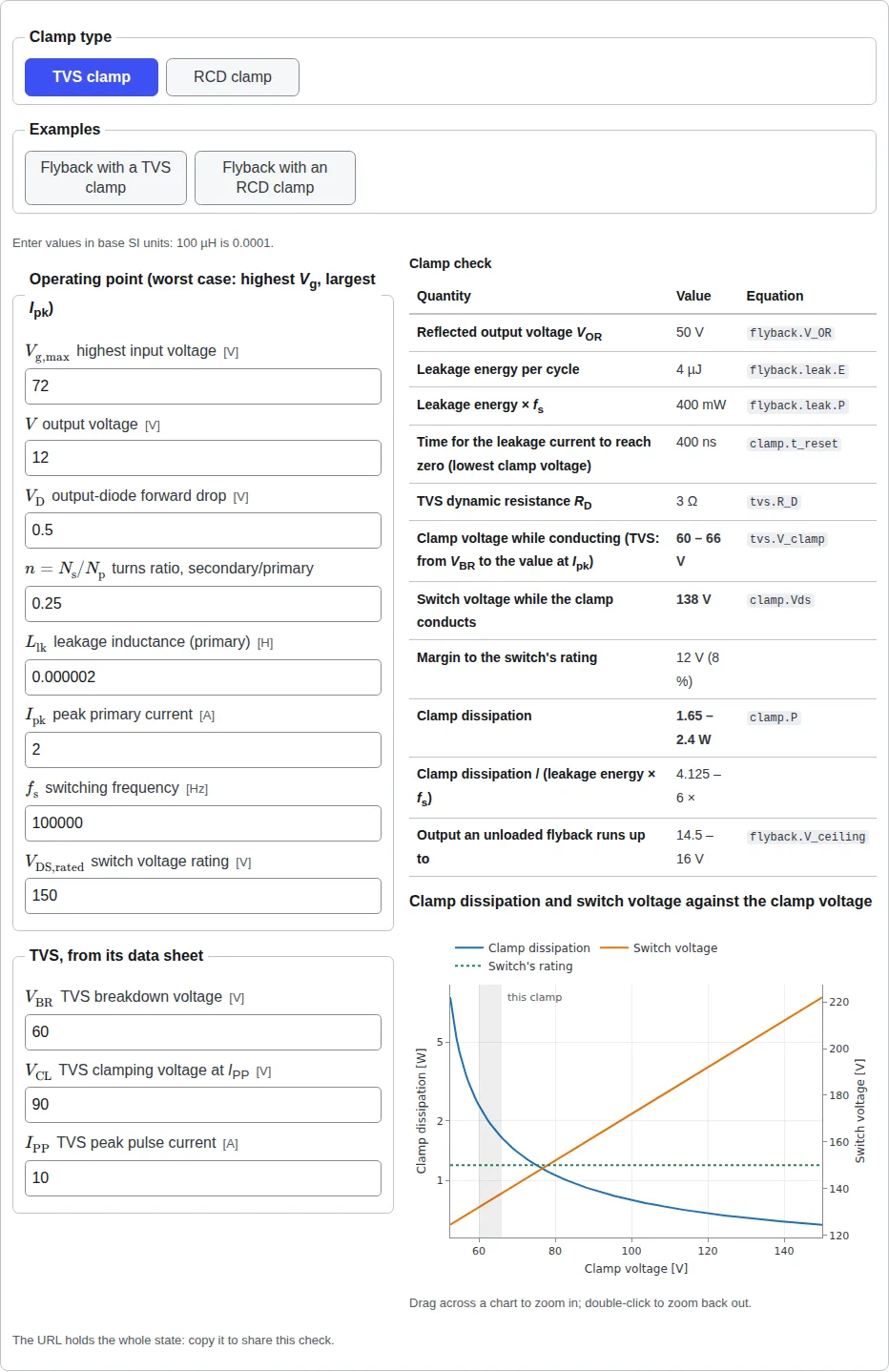
The numbers in the examples, presets and exercises on this site are synthetic: round teaching values, not data from any real design.