Converter designer
Pick a topology and give the input-voltage range, the output voltage, the full-load power, the lightest load that must stay in CCM, the switching frequency and two ripple targets. The designer gives:
- the duty-ratio range;
- the inductance for the current-ripple target and the one that keeps the lightest load in CCM;
- the output capacitance for the voltage-ripple target;
- the ripple, the peak current and the switch and diode voltages at the worst point of the input range;
- against over the duty-ratio range.
Each result names the catalogue equation it comes from. The links under the results open the simulator with the designed parts at either end of the input range, to check the design in the time domain; the parts there are ideal, apart from the flyback’s diode drop. Other links open the loss budget at the same points, with the switch and diode data of its example and no core data, because the designer does not size the core.
How it sizes the converter
Section titled “How it sizes the converter”The designer examines a grid of input voltages across the range, plus the points inside the range where a quantity peaks, and keeps the worst case of each result. It uses only catalogue equations. Where it needs an equation solved for one of its inputs (the duty ratio, an inductance, a capacitance), it finds that value by bisection on the catalogue’s own evaluator, so the tool and the theory pages cannot disagree.
- Duty ratio. The CCM conversion ratio is solved for at each input voltage: buck, boost, buck-boost, flyback and forward. For the flyback the diode drop adds to the output voltage, as in the volt-second balance behind the critical input voltage.
- Inductance for the ripple target. At full load the average inductor current (buck, boost, buck-boost, and the flyback’s magnetizing current) times the ripple target gives the allowed ripple, and the ripple equation (buck, boost, buck-boost, flyback, forward) is solved for the inductance. The forward converter’s output stage is a buck converter fed with , so its output inductor carries the load current [Erickson & Maksimović 2020, Ch. 6].
- Inductance for CCM at the lightest load. The critical inductance at the lightest load, with the largest over the duty-ratio range (buck and forward, boost, buck-boost, flyback). For the flyback the diode drop again adds to the output voltage, at the same output current, so the load here is the one that draws that current at the output voltage plus the diode drop; with the load itself, the boundary would come out too low.
- Inductance used. The larger of the two, unless you enter one. With it, (definition) at full load and at the lightest load (for the flyback, with the load of step 3) is compared with in the chart: the converter is in CCM where lies above the curve.
- Ripple and stresses. The ripple with the inductance used, the peak current, and the switch voltage (buck, boost, buck-boost, flyback, forward). In the buck, boost and buck-boost the diode blocks the same voltage as the switch [Erickson & Maksimović 2020, Ch. 6]; the flyback’s diode blocks its own reverse voltage.
- Output capacitance. The voltage-ripple equation is solved for : buck and forward, boost, buck-boost, flyback.
For the forward converter, the tool also checks the duty ratio against the reset limit.
Ripple targets
Section titled “Ripple targets”Both targets are ratios of the half peak-to-peak ripple, the convention of the catalogue [Erickson & Maksimović 2020, Ch. 2]: the current target is the inductor-current ripple over the average inductor current at full load (the magnetizing current for the flyback), and the voltage target is the output-voltage ripple over the output voltage.
Limitations
Section titled “Limitations”- Ideal parts. Switches, diodes (except the flyback’s diode drop), inductors and capacitors are ideal. A capacitor’s series resistance adds a ripple of its own (ESR ripple), so the capacitance found here is a lower bound.
- CCM designs only. The duty ratios and ripples assume CCM, and the inductance is sized for CCM; a converter designed to run in DCM (a DCM flyback, for example) is not sized here. Where the full load runs in DCM, the designer says so, and the DCM equations apply there instead.
- Not sized here. Ratings and thermal limits are not checked, and neither are the forward converter’s magnetizing inductance and reset winding. Check the design in the simulator, and estimate its losses with the loss budget.
Screenshot
Section titled “Screenshot”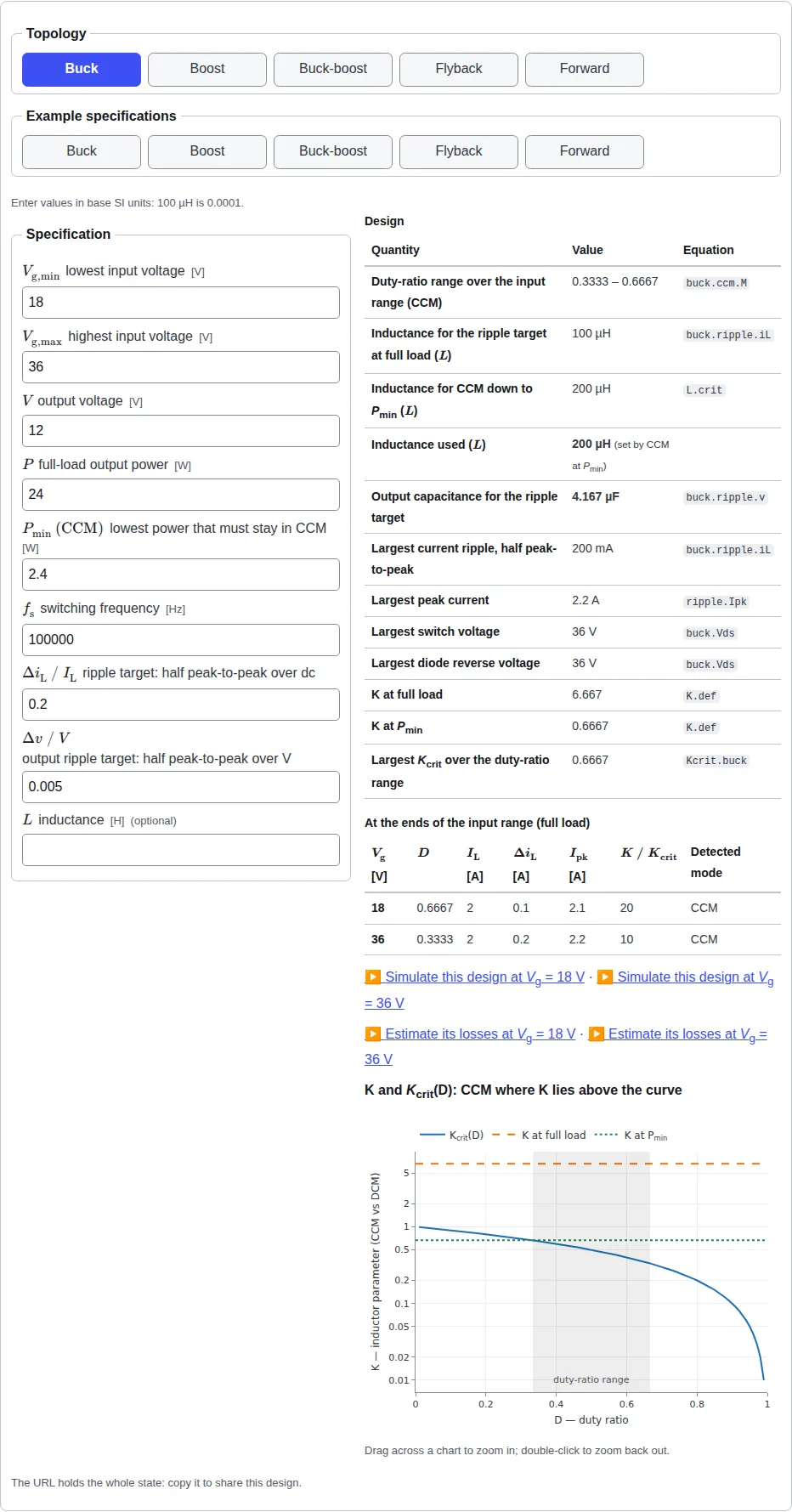
The numbers in the examples, presets and exercises on this site are synthetic: round teaching values, not data from any real design.