Sense chain
A converter measures its current with a shunt resistor, whose small voltage an amplifier raises for an ADC. Each stage sets a limit. The shunt takes voltage and power from the circuit it measures. The amplifier runs out of output range at the top, and adds its offset at the bottom. The pads and solder in the sense path add resistance of their own, and the ADC folds anything above half its sampling rate back into the reading. The sense chain takes the whole chain, in SI units, from zero to the largest current:
- the gain, the full-scale current and which limit sets it, and the output floor, each at the worst case of the offset and the pad resistance;
- the sense voltage (the burden) and the shunt’s dissipation at the largest current;
- the offset-equivalent current, the pad error, and the error of the reading at the smallest current;
- the R-C filter’s corner against the Nyquist frequency.
It flags each violation, and each result names the equations it comes from. Two charts show the output and the relative error against the current.
What it computes
Section titled “What it computes”The tool measures currents from zero up to , and is the error you accept at the smallest current that matters, .
Sense voltage and burden
Section titled “Sense voltage and burden”By Ohm’s law the shunt turns the current into the sense voltage
[Alexander & Sadiku 2017, Ch. 2](sense voltage, on the current sensing page).
This voltage is the amplifier’s signal, and also the burden: the voltage the shunt takes from the circuit it measures. A larger shunt gives a larger signal, and costs more burden and more dissipation, the shunt’s conduction loss at the largest current. The tool compares them with the circuit’s allowance and the shunt’s power rating when you enter them.
The amplifier’s output
Section titled “The amplifier’s output”A current-output amplifier forces the sense voltage across its input resistor . The resulting current flows out through , which turns it back into a voltage to ground [Analog Devices, LTC6101/LTC6101HV]:
- sense-amplifier output
- current through the shunt
- gain-setting input resistor
- output resistor
- sense (shunt) resistor
Assumptions, convention and source
- Assumptions
- ideal amplifier (no offset, gain error or output headroom limit)
- Notes
- the amplifier forces across and sends that current through ; the output headroom limit is set by the supply, not by the gain
- Source
- Analog Devices, LTC6101/LTC6101HV
- Derivation
- step-by-step sympy derivation
- Equation id
sense.current_out_monitor· equations.yaml entry
The two resistors set the gain.
A voltage-output amplifier has a fixed gain , and adds the voltage on its REF pin [Texas Instruments 2023, Equation 1]:
- sense-amplifier output
- amplifier gain
- current through the shunt
- sense (shunt) resistor
- REF-pin voltage
Assumptions, convention and source
- Assumptions
- ideal amplifier (no offset, gain error or output headroom limit)
- Notes
- the amplifier multiplies the sense voltage by its gain and adds the REF voltage, so a current of either sign swings the output either side of ; the output cannot quite reach the supply rails
- Source
- Texas Instruments 2023, Equation 1, from its definitions of the load current, the sense resistor, the gain and the REF voltage
- Derivation
- step-by-step sympy derivation
- Equation id
sense.voltage_out_monitor· equations.yaml entry
The REF voltage sets the output at zero current. A current of either sign then swings the output to either side of it, and a REF voltage of zero suits a current that flows one way only [Texas Instruments 2023].
Offset
Section titled “Offset”The amplifier’s input offset voltage adds directly to the sense voltage [Analog Devices, LTC6101/LTC6101HV, Applications Information]. So the output reads it as a current, the same at every current:
- offset-equivalent current
- sense (shunt) resistor
- amplifier input offset
Assumptions, convention and source
- Assumptions
- the amplifier's input offset voltage is its only error (no gain error, no bias current)
- Notes
- the offset adds directly to the sense voltage, so the output reads it as this current: the error floor at small currents; a larger sense resistor lowers it
- Source
- Analog Devices, LTC6101/LTC6101HV, Applications Information: output error due to the amplifier's DC offset voltage; Texas Instruments 2023, selecting the current-sense resistor
- Derivation
- step-by-step sympy derivation
- Equation id
sense.offset_current· equations.yaml entry
A larger shunt lowers this current, because the same current then gives a larger sense voltage [Texas Instruments 2023]. The price is more burden and more dissipation.
Pad and solder resistance
Section titled “Pad and solder resistance”With a shunt of a few milliohms or less, the resistance of the solder becomes a substantial part of the sense element’s resistance, and adds to the measurement error [O'Sullivan 2012]. If the sense connections sit beyond the pads, the amplifier sees the load current through the shunt and the pads together, . So the reading is high by the same fraction at every current (pad error, see current sensing).
A Kelvin connection takes the pads out of the sense path: a four-terminal shunt, or a two-terminal one on a four-pad (split-pad) layout [O'Sullivan 2012]. The LTC6101 data sheet recommends Kelvin connections to the sense resistor in all but the lowest-power applications [Analog Devices, LTC6101/LTC6101HV, Applications Information]. With a Kelvin connection, enter as zero.
What the amplifier reads
Section titled “What the amplifier reads”With both the offset and the pad resistance, the amplifier sees the load current through the shunt and the pads, plus its offset, and reads the sum as a current through the shunt alone:
- current the reading indicates
- current through the shunt
- sense (shunt) resistor
- pad and solder resistance
- amplifier input offset
Assumptions, convention and source
- Assumptions
- the amplifier's input offset voltage is its only error (no gain error, no bias current)
- Notes
- the amplifier sees and treats it as , so its output is the output equation taken at ; with the offset's sign that raises it, this bounds the output from above, with the other sign from below
- Source
- Analog Devices, LTC6101/LTC6101HV, Applications Information: output error due to the amplifier's DC offset voltage; derived here; O'Sullivan 2012, solder resistance of milliohm shunts
- Derivation
- step-by-step sympy derivation
- Equation id
sense.reading· equations.yaml entry
The output is the output equation taken at this current. A data sheet gives the offset’s largest magnitude, not its sign, so the tool takes both signs: the one that raises the output for the upper limits, and the one that lowers it for the floor.
Error at the smallest current
Section titled “Error at the smallest current”Relative to the true current, the two errors add, with no cross term:
- relative error of the reading
- current through the shunt
- sense (shunt) resistor
- pad and solder resistance
- amplifier input offset
Assumptions, convention and source
- Assumptions
- the amplifier's input offset voltage is its only error (no gain error, no bias current)
- Notes
- the two errors add exactly: the offset's share falls in inverse proportion to the current, so it sets the error at the smallest current, while the pad's share is the same at every current
- Source
- Analog Devices, LTC6101/LTC6101HV, Applications Information: output error due to the amplifier's DC offset voltage; derived here; O'Sullivan 2012, solder resistance of milliohm shunts
- Derivation
- step-by-step sympy derivation
- Equation id
sense.rel_error· equations.yaml entry
The offset’s part falls in inverse proportion to the current, so it matters most at . The pad’s part is the same at every current. The tool flags each part that alone exceeds at , and flags the sum when only the two together do. The error chart plots both against the current, with the target.
Full scale and the output floor
Section titled “Full scale and the output floor”Two limits cap the output. The amplifier delivers only up to its largest output voltage , which depends on its supply; the ADC reads only up to its full scale . A voltage-output amplifier’s data sheet gives its output swing as a small voltage short of the supply rail and above ground [Texas Instruments 2023]. The LTC6101 data sheet gives its largest output as absolute values at stated supply voltages [Analog Devices, LTC6101/LTC6101HV]. Enter the values that apply at your supply.
The tool takes the highest output, with the pad resistance and the offset at the sign that raises it, and solves for the current at which it reaches the lower of the two limits: that is the full-scale current. If it lies below , the reading can clip before the largest current. If it lies far above, the ADC’s range is partly wasted; the table gives the share of the full scale that the highest output at uses.
At the bottom, a voltage-output amplifier with its REF pin at zero cannot drive its output all the way to ground. Its lowest output , the swing to ground, sets a floor: every current whose output would fall below it reads the same. An offset of the sign that lowers the output holds the output at the floor up to a current of its own. The tool takes the lowest output, gives the current below which it can stay at the floor, and flags a floor above . A REF voltage above the floor removes it.
Filter and sampling
Section titled “Filter and sampling”An ADC that samples at the rate represents the band from dc to the Nyquist frequency:
- Nyquist frequency
- ADC sampling rate
Assumptions, convention and source
- Assumptions
- uniform sampling at a fixed rate
- definition
- Notes
- the Nyquist bandwidth runs from dc to ; any component above it aliases back into that band, so an anti-aliasing filter removes it before the ADC
- Source
- Kester, What the Nyquist Criterion Means to Your Sampled Data System Design
- Equation id
adc.nyquist· equations.yaml entry
Any component above it aliases back into that band, so an anti-aliasing filter removes it before the ADC [Kester, What the Nyquist Criterion Means to Your Sampled Data System Design]. In a converter, the switching ripple is such a component. The tool takes a first-order R-C filter, with its corner frequency and gain magnitude from the phasors page. It flags a corner at or above the Nyquist frequency, and gives the filter’s gain at the Nyquist frequency. That check is the tool’s own rule, built on the Nyquist criterion. A single pole attenuates only in inverse proportion to the frequency, so a corner below the Nyquist frequency is the least to ask for, and not always enough: the gain at the Nyquist frequency tells how much still passes there.
A current-output amplifier’s output is a current source, and turns it into a voltage. Seen from the filter, that is a source with behind it, its Thevenin equivalent [Alexander & Sadiku 2017, Ch. 4]. So the filter’s capacitor sees in series with (the derivation is linked under the equation):
- resistance the filter capacitor sees
- output resistor
- filter resistor
Assumptions, convention and source
- Assumptions
- ideal amplifier (no offset, gain error or output headroom limit)
- first-order R-C low-pass filter with no load on its output
- Notes
- the amplifier's output is a current source loaded by ; its Thevenin equivalent puts in series with , so the capacitor sees both and the corner frequency is lower than alone gives; with no load on the filter the dc output stays
- Source
- Alexander & Sadiku 2017, Ch. 4 (Circuit Theorems: Thevenin's and Norton's theorems); derived here
- Derivation
- step-by-step sympy derivation
- Equation id
sense.filter_R· equations.yaml entry
A capacitor straight across , with no , is a filter of this kind too. The tool takes a voltage-output amplifier’s output as an ideal voltage source, so there the capacitor sees alone; a real amplifier’s output resistance adds to .
Enter the converter’s switching frequency if you know it: the table then gives the filter’s gain there, the share of the switching ripple that reaches the ADC.
Worked examples
Section titled “Worked examples”A current-output amplifier on a two-terminal shunt:
| Symbol | Value | How it is obtained |
|---|---|---|
| current through the shunt | 2 A | given |
| smallest current to measure | 200 mA | given |
| sense (shunt) resistor | 10 mΩ | given |
| pad and solder resistance | 500 µΩ | given |
| gain-setting input resistor | 100 Ω | given |
| output resistor | 10 kΩ | given |
| amplifier input offset | 100 µV | given |
| amplifier's lowest output | 0 V | given |
| amplifier's largest output | 4 V | given |
| ADC full-scale input | 2.5 V | given |
| ADC sampling rate | 10 kHz | given |
| filter resistor | 1 kΩ | given |
| filter capacitor | 10 nF | given |
| relative error target (0.01 = 1 %) | 0.01 | given |
| voltage across the shunt | 20 mV | Voltage across a current-sense resistor |
| sense-amplifier output | 2 V | Output of a current-output high-side current-sense amplifier |
| current the reading indicates | 2.11 A | Current a shunt reading indicates, with the pad resistance and the offset |
| highest output (worst case) | 2.11 V | Output of a current-output high-side current-sense amplifier |
| offset-equivalent current | 10 mA | Current equivalent to a sense amplifier's input offset voltage |
| error from pad resistance | 0.05 | Gain error from pad and solder resistance in a shunt's sense path |
| relative error of the reading | 0.1 | Relative error of a shunt reading from the offset and the pad resistance |
| resistance the filter capacitor sees | 11 kΩ | Resistance an R-C filter's capacitor sees behind a current-output sense amplifier |
| corner (-3 dB) frequency | 1.45 kHz | Corner frequency of a first-order R-C low-pass filter |
| Nyquist frequency | 5 kHz | Nyquist frequency of a sampled signal |
| low-pass gain | 0.278 | Gain magnitude of a first-order low-pass filter |
Operating mode: At I_min the reading misses the error target (: does not hold) The filter's corner lies below the Nyquist frequency (: holds)
At the largest current the output reaches 2 V nominally. With the pad resistance and the offset, the amplifier reads 2.11 A, and its output can reach 2.11 V: still below the ADC’s full scale of 2.5 V. The low end is the problem. The offset-equivalent current, 10 mA, and the pad error, 0.05, put the reading at 200 mA off by a fraction of 0.1, against a target of 0.01. A Kelvin connection removes the pad’s part. The offset’s part needs a larger shunt or an amplifier with a lower offset. The filter’s capacitor sees 11 kΩ, plus , which puts its corner below the Nyquist frequency.
A voltage-output amplifier on a Kelvin-connected shunt:
| Symbol | Value | How it is obtained |
|---|---|---|
| current through the shunt | 5 A | given |
| smallest current to measure | 500 mA | given |
| sense (shunt) resistor | 5 mΩ | given |
| pad and solder resistance | 0 Ω | given |
| amplifier gain | 100 | given |
| REF-pin voltage | 0 V | given |
| amplifier input offset | 20 µV | given |
| amplifier's lowest output | 10 mV | given |
| amplifier's largest output | 3.2 V | given |
| ADC full-scale input | 3.3 V | given |
| ADC sampling rate | 20 kHz | given |
| filter resistor | 100 Ω | given |
| filter capacitor | 1 µF | given |
| relative error target (0.01 = 1 %) | 0.01 | given |
| voltage across the shunt | 25 mV | Voltage across a current-sense resistor |
| sense-amplifier output | 2.5 V | Output of a fixed-gain voltage-output current-sense amplifier |
| current the reading indicates | 5 A | Current a shunt reading indicates, with the pad resistance and the offset |
| highest output (worst case) | 2.5 V | Output of a fixed-gain voltage-output current-sense amplifier |
| offset-equivalent current | 4 mA | Current equivalent to a sense amplifier's input offset voltage |
| relative error of the reading | 0.008 | Relative error of a shunt reading from the offset and the pad resistance |
| corner (-3 dB) frequency | 1.59 kHz | Corner frequency of a first-order R-C low-pass filter |
| Nyquist frequency | 10 kHz | Nyquist frequency of a sampled signal |
| low-pass gain | 0.157 | Gain magnitude of a first-order low-pass filter |
Operating mode: At I_min the reading meets the error target (: holds) The filter's corner lies below the Nyquist frequency (: holds)
The highest output at the largest current, 2.5 V, stays below the amplifier’s largest output of 3.2 V, and the error at the smallest current, 0.008, meets the target. The filter’s corner, 1.59 kHz, lies below the Nyquist frequency of 10 kHz. At that frequency the filter still passes a fraction 0.157 of the signal.
Limitations
Section titled “Limitations”- Offset and pads only. The error model has the amplifier’s input offset and the pad resistance. It leaves out the amplifier’s gain error, the tolerance of the gain resistors, the input bias currents, the common-mode rejection and noise. It also leaves out the shunt’s own tolerance and its change with temperature, and the ADC’s own errors. A real error budget adds them.
- Currents from zero up. The chain is checked for a current that flows one way. The shunt’s dissipation is that of a dc current at . A varying current dissipates by its rms value, while the output limits apply to its peak.
- Output limits as entered. The output range depends on the supply, the load and the temperature. Take the data sheet’s limits at your conditions.
- An unloaded first-order filter. The ADC’s input draws charge when it samples. Its data sheet gives the source impedance it allows.
- One pad resistance. For the lowest-value shunts, where the sense point sits on the pad and how evenly the current spreads through the resistor matter too [O'Sullivan 2012].
Screenshot
Section titled “Screenshot”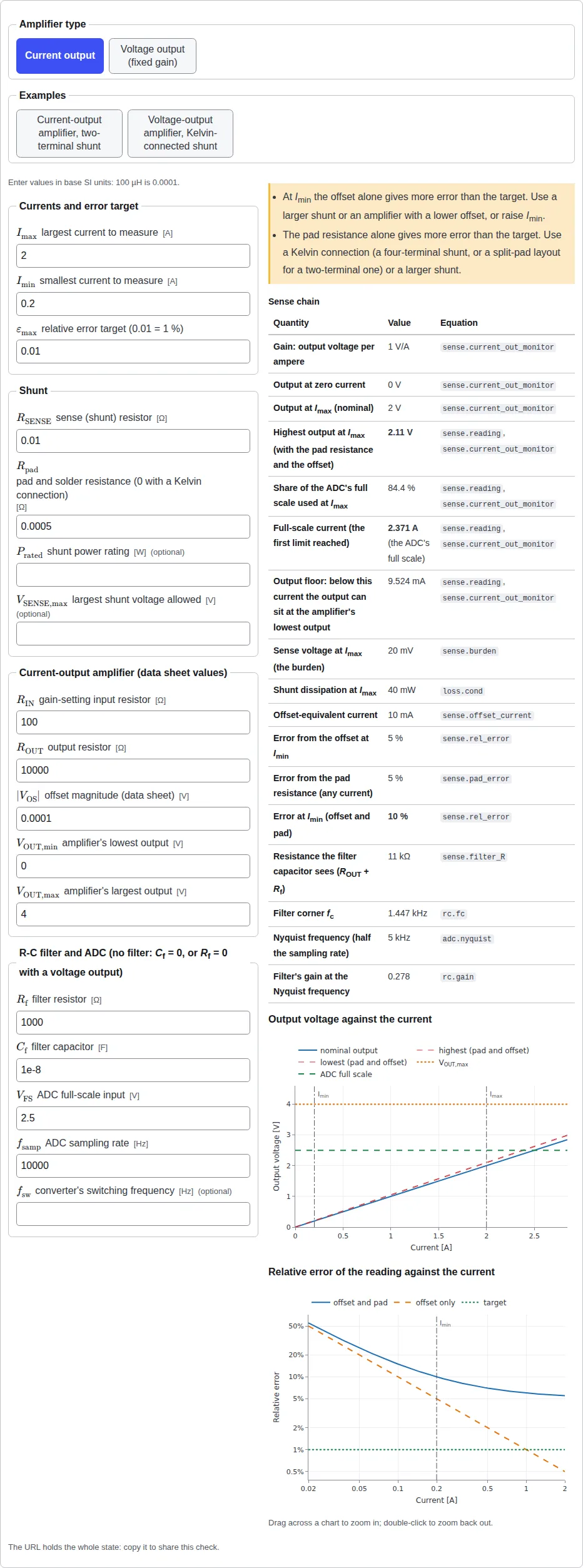
The numbers in the examples, presets and exercises on this site are synthetic: round teaching values, not data from any real design.