Magnetics designer
Pick an inductor or a flyback transformer, a core and the windings. The two table cores carry the values TDK publishes for them in its N87 ferrite [TDK Electronics, E 25/13/7 (EF 25)], [TDK Electronics, ETD 29/16/10]. For any other core, choose “Other core” and enter the values from its data sheet. The designer gives:
- the fewest turns that keep the peak flux density within a limit, and the air gap that then gives the inductance;
- for a table core, the gapped core sets its data sheet offers, with the turns each one needs;
- the peak flux density, and the ac flux amplitude that the core loss depends on;
- the window utilization, and each winding’s dc resistance and ac resistance factor at the switching frequency;
- for a flyback, the leakage inductance of the winding arrangement.
Each result names its equation. The chart shows each winding’s ac resistance factor against frequency.
What it computes
Section titled “What it computes”Enter the inductance and the peak and rms current of the winding. For a flyback these are the magnetizing inductance referred to the primary and the primary’s currents, and the secondary’s rms current is entered separately. The converter designer gives the inductance and the peak current. The ripple is half the peak-to-peak ripple, as everywhere on this site. is the largest flux density the design allows: below the material’s saturation flux density at the core’s highest temperature, with a margin [Erickson & Maksimović 2020, Ch. 11].
The flux density follows the current (peak flux density). Holding its peak at gives the fewest turns [Erickson & Maksimović 2020, Ch. 11]:
- number of turns
- effective core area
- largest flux density allowed
- peak current
- inductance
Assumptions, convention and source
- Assumptions
- linear (unsaturated) magnetic material
- flux density uniform over A_e
- Notes
- more turns lower the peak flux density at the same inductance and current, but lengthen the winding and raise its resistance
- Source
- Erickson & Maksimović 2020, Ch. 11 (Inductor Design); derived here
- Derivation
- step-by-step sympy derivation
- Equation id
mag.N_Bmax· equations.yaml entry
The tool evaluates it at the core’s smallest cross-section , where the flux density is highest, and rounds up to whole turns. More turns lower the flux density further, but lengthen the winding and raise its resistance. Enter to use more.
The gap
Section titled “The gap”With the turns fixed, the inductance sets the gap. The magnetic circuit of a gapped core (inductance factor of a gapped core), solved for the gap length, gives:
- air-gap length
- effective core area
- inductance
- number of turns
- effective magnetic path length
- initial relative permeability
- permeability of free space
Assumptions, convention and source
- Assumptions
- linear (unsaturated) magnetic material
- no fringing flux at the gap
- flux density uniform over A_e
- Notes
- a negative result means the ungapped core already gives less than this inductance with N turns: more turns are needed; fringing lets a real gap be somewhat longer than this estimate
- Source
- Erickson & Maksimović 2020, Ch. 11 (Inductor Design); derived here
- Derivation
- step-by-step sympy derivation
- Equation id
mag.gap_length· equations.yaml entry
Here is the effective permeability of the ungapped set. The tool takes it from the data sheet’s of the ungapped set, through the same equation with no gap. A negative result means that even the ungapped core gives less than the inductance with these turns: add turns.
This estimate ignores fringing. Around the gap the flux spreads beyond the core’s area, so a real gap passes more flux than the estimate assumes, and it must be longer for the same inductance. A data sheet therefore gives the of its gapped core sets, each a gapped core with an ungapped one [TDK Electronics, E 25/13/7 (EF 25)]. For a table core the tool lists these sets. For each it shows the turns that give the inductance, the inductance of those whole turns and the peak flux density at . The button in a row uses its turns. Use a set with a large gap, and compare its gap with the tool’s estimate for those turns: the real gap is clearly longer.
Flux density and its swing
Section titled “Flux density and its swing”The peak flux density at is what must stay below saturation. The core loss depends on the swing instead. A ripple of moves the flux density about its dc value by:
- ac flux-density amplitude
- effective core area
- inductor ripple, half peak-to-peak
- inductance
- number of turns
Assumptions, convention and source
- Assumptions
- linear (unsaturated) magnetic material
- flux density uniform over A_e
- Convention
- is half the peak-to-peak ripple (Erickson), so is half the peak-to-peak swing : the amplitude that core-loss data take
- Notes
- the flux density follows the current, so the ripple alone sets its swing, the quantity core-loss data are given for; the dc current sets where the swing lies, and with it the margin to saturation ()
- Source
- Erickson & Maksimović 2020, Ch. 10 (Basic Magnetics Theory); derived here
- Derivation
- step-by-step sympy derivation
- Equation id
mag.B_ac· equations.yaml entry
This is the amplitude that core-loss data take (core loss per volume): read the loss per volume off the material’s loss curves at and , or use the loss budget. In a CCM inductor the ripple is a small part of the current, and so is of . In a DCM flyback the current falls to zero every period, and the swing is the whole peak.
Copper and the window
Section titled “Copper and the window”Each winding is round wire: strands in parallel, each of bare diameter and diameter over its insulation, wound in layers across the coil former’s winding breadth . The copper of one turn, and the part of the window that all windings fill:
- bare conductor area of one turn
- bare wire diameter
- strands in parallel
Assumptions, convention and source
- Assumptions
- definition
- Notes
- the bare diameter, without the insulation; wire tables give both
- Source
- National Bureau of Standards 1966
- Equation id
wind.round_area· equations.yaml entry
- window utilization
- bare conductor area of one turn
- number of turns
- winding window area
Assumptions, convention and source
- Assumptions
- definition
- Notes
- insulation, the bobbin and the gaps between round wires leave only part of the window to copper; a design keeps K_u below what it can wind
- Source
- Erickson & Maksimović 2020, Ch. 11 (Inductor Design)
- Equation id
wind.fill· equations.yaml entry
must stay below what can actually be wound. Insulation, the coil former and the gaps between round wires take the rest [Erickson & Maksimović 2020, Ch. 11]. The tool warns above .
DC resistance
Section titled “DC resistance”Copper’s resistivity rises with temperature. For annealed copper the tool uses the values of the NBS copper wire tables [National Bureau of Standards 1966]:
- conductor resistivity
- winding temperature
- temperature coefficient at 20 °C
- resistivity at 20 °C
Assumptions, convention and source
- Assumptions
- resistance linear in temperature near 20 °C
- Notes
- for annealed copper and per kelvin; a winding at 100 °C has about 31 % more resistance than at 20 °C
- Source
- National Bureau of Standards 1966
- Equation id
wind.rho_T· equations.yaml entry
- winding dc resistance
- bare conductor area of one turn
- mean length per turn
- number of turns
- conductor resistivity
Assumptions, convention and source
- Assumptions
- a dc current spread uniformly over the conductor's cross-section
- Notes
- the winding is a conductor long; the resistivity of copper rises with temperature
- Source
- Erickson & Maksimović 2020, Ch. 11 (Inductor Design); derived here
- Derivation
- step-by-step sympy derivation
- Equation id
wind.dcr· equations.yaml entry
(conduction loss) is the loss the current would cause if it were dc. The ac part of the current adds to it, as the next section shows.
AC resistance (Dowell)
Section titled “AC resistance (Dowell)”At high frequency the current crowds into a surface layer about a skin depth thick [Erickson & Maksimović 2020, Ch. 10]:
- skin depth
- frequency
- conductor resistivity
- permeability of free space
Assumptions, convention and source
- Assumptions
- a good conductor carrying a sinusoidal current (displacement current neglected)
- Notes
- the current density falls by a factor for every skin depth into the conductor; conductors much thicker than carry the current in a surface layer
- Source
- Erickson & Maksimović 2020, Ch. 10 (Basic Magnetics Theory: eddy currents in winding conductors); derived here
- Derivation
- step-by-step sympy derivation
- Equation id
wind.skin_depth· equations.yaml entry
In a winding of several layers, each layer also carries the field of the layers below it, which induces eddy currents in it: the proximity effect. Dowell’s analysis treats each layer as a foil [Dowell 1966]. For round wire, each strand becomes a square of the same area, and the layer becomes a foil of that thickness whose gaps lower its conductivity [Erickson & Maksimović 2020, Ch. 10]:
- porosity of a layer
- turns per layer
- winding breadth
- bare wire diameter
- strands in parallel
Assumptions, convention and source
- Assumptions
- each round conductor replaced by a square conductor of the same area, the layer by a foil of that thickness
- Notes
- a square of side has the strand's area; a layer whose squares fill the whole breadth has porosity 1, and a value above 1 means the turns do not fit in the layer
- Source
- Dowell 1966; Erickson & Maksimović 2020, Ch. 10 (Basic Magnetics Theory: foil windings and layers)
- Equation id
wind.porosity· equations.yaml entry
- layer thickness over skin depth
- bare wire diameter
- skin depth
- porosity of a layer
Assumptions, convention and source
- Assumptions
- each round conductor replaced by a square conductor of the same area, the layer by a foil of that thickness
- Notes
- the equivalent foil is thick; its gaps lower its effective conductivity by the porosity, which enters as
- Source
- Dowell 1966; Erickson & Maksimović 2020, Ch. 10 (Basic Magnetics Theory: foil windings and layers)
- Equation id
wind.phi_round· equations.yaml entry
- ac resistance factor
- layers from zero to peak MMF
- layer thickness over skin depth
Assumptions, convention and source
- Assumptions
- foil layers spanning the winding breadth, a sinusoidal current, and a one-dimensional field in the window
- Notes
- the first term is the skin effect in each layer, the second the proximity effect of the layers' fields on each other, growing as ; with well below 1 the factor tends to 1
- Source
- Dowell 1966; Erickson & Maksimović 2020, Ch. 10 (Basic Magnetics Theory: eddy currents in winding conductors)
- Equation id
wind.dowell· equations.yaml entry
is the ratio of the ac resistance to at one frequency. Each harmonic of the current sees the factor at its own frequency, so the chart plots against frequency, with marked. With above 1, each added layer raises steeply, as . The remedies are fewer layers of thinner strands in parallel, or a foil.
In an inductor with a small ripple, the ac part of the current is small and matters little: the table’s dc loss is then most of the copper loss. A flyback’s windings carry pulses, so much of each winding’s rms current is ac. Its harmonics see at their frequencies, and the copper loss can be several times the dc loss.
Leakage inductance (flyback)
Section titled “Leakage inductance (flyback)”The field between the windings stores energy that does not couple them: the leakage inductance. With the secondary wound over the primary (P-S):
- leakage inductance (primary)
- mean length per turn
- number of turns
- winding breadth
- spacing between the windings
- primary winding height
- secondary winding height
- permeability of free space
Assumptions, convention and source
- Assumptions
- one-dimensional field in the winding window: the MMF changes only across the layers, and the field runs along the winding breadth
- Notes
- referred to the primary; each winding counts with a third of its height and the spacing in full, and a broad, low window gives the least leakage
- Source
- Erickson & Maksimović 2020, Ch. 10 (Basic Magnetics Theory: leakage flux in windings, MMF diagrams); derived here
- Derivation
- step-by-step sympy derivation
- Equation id
xfmr.leakage.ps· equations.yaml entry
Splitting the primary into two halves around the secondary (P-S-P) halves the peak magnetomotive force in the window, and the leakage falls to about a quarter [Erickson & Maksimović 2020, Ch. 10]:
- leakage inductance (primary)
- mean length per turn
- number of turns
- winding breadth
- spacing between the windings
- primary winding height
- secondary winding height
- permeability of free space
Assumptions, convention and source
- Assumptions
- one-dimensional field in the winding window: the MMF changes only across the layers, and the field runs along the winding breadth
- Notes
- splitting the primary halves the peak MMF, so the stored energy, and with it the leakage, falls to about a quarter
- Source
- Erickson & Maksimović 2020, Ch. 10 (Basic Magnetics Theory: interleaving the windings); derived here
- Derivation
- step-by-step sympy derivation
- Equation id
xfmr.leakage.psp· equations.yaml entry
The tool takes a winding’s height as its layers times , and as the insulation between two windings (for P-S-P, at each of the two interfaces). In a flyback the leakage energy goes to the clamp: take this inductance to the clamp check.
Worked examples
Section titled “Worked examples”A buck inductor on the E 25/13/7 set:
| Symbol | Value | How it is obtained |
|---|---|---|
| inductance | 100 µH | given |
| peak inductor current | 2.2 A | given |
| rms inductor current | 2 A | given |
| inductor ripple, half peak-to-peak | 200 mA | given |
| switching frequency | 100 kHz | given |
| largest flux density allowed | 300 mT | given |
| winding temperature | 100 °C | given |
| winding breadth | 15 mm | given |
| largest window utilization that can be wound | 0.4 | given |
| bare wire diameter | 0.8 mm | given |
| wire diameter over its insulation | 0.86 mm | given |
| strands in parallel | 1 | given |
| layers of the winding (Dowell's M) | 1 | given |
| effective core area | 52.5 mm² | TDK Electronics, E 25/13/7 (EF 25) |
| smallest cross-section of the core | 51.5 mm² | TDK Electronics, E 25/13/7 (EF 25) |
| effective magnetic path length | 57.5 mm | TDK Electronics, E 25/13/7 (EF 25) |
| inductance factor of the ungapped set | 1.85 µH | TDK Electronics, E 25/13/7 (EF 25) |
| winding window area | 61 mm² | TDK Electronics, E 25/13/7 (EF 25) |
| mean length per turn | 50 mm | TDK Electronics, E 25/13/7 (EF 25) |
| fewest turns for Bmax, at Amin | 14.24 | Fewest turns that keep the peak flux density at a limit |
| number of turns | 15 | rounded up |
| inductance factor the design needs | 444.4 nH | Inductance from the inductance factor |
| effective permeability of the ungapped set | 1612 | Inductance factor of a gapped core |
| gap, without fringing | 0.1128 mm | Air-gap length that gives an inductance with N turns |
| peak flux density (at Amin) | 284.8 mT | Peak flux density from inductance and peak current |
| ac flux-density amplitude | 25.4 mT | AC flux-density amplitude from the current ripple |
| conductor resistivity (at Tw) | 22.66 nΩ·m | Resistivity of a conductor at its temperature |
| skin depth (at fs) | 0.2396 mm | Skin depth of a conductor |
| bare conductor area of one turn | 0.5027 mm² | Copper area of one turn of round strands |
| winding dc resistance | 33.81 mΩ | DC resistance of a winding |
| porosity of a layer | 0.709 | Porosity of a layer of round conductors |
| layer thickness over skin depth | 2.492 | Dowell's layer thickness for round conductors |
| ac resistance factor (at fs) | 2.468 | AC resistance factor of a foil winding (Dowell) |
| loss at the dc resistance | 135.3 mW | Conduction loss in a resistance |
| window utilization | 0.1236 | Window utilization of a winding |
The fewest turns need a gap that no set of the data sheet has. In the tool’s table of gapped sets, the smallest gap needs as many turns but gives more inductance, so its peak flux density exceeds . The next set stays within it with a few more turns. One layer of this wire has an well above 1 at the switching frequency, from the skin effect alone, but only the small ripple sees it.
A flyback transformer on the ETD 29/16/10 set, wound P-S. Its operating point is the converter designer’s flyback example at its lowest input voltage, with the inductance set to its ripple target:
| Symbol | Value | How it is obtained |
|---|---|---|
| magnetizing inductance (primary) | 600 µH | given |
| peak primary current | 1.37 A | given |
| rms primary current | 914 mA | given |
| magnetizing ripple, half peak-to-peak | 174 mA | given |
| switching frequency | 100 kHz | given |
| largest flux density allowed | 300 mT | given |
| turns ratio, secondary/primary | 0.25 | given |
| rms secondary current | 3.1 A | given |
| winding temperature | 100 °C | given |
| winding breadth | 19 mm | given |
| largest window utilization that can be wound | 0.4 | given |
| spacing between the windings | 0.1 mm | given |
| bare wire diameter (primary) | 0.5 mm | given |
| wire diameter over its insulation (primary) | 0.56 mm | given |
| strands in parallel (primary) | 1 | given |
| layers of the winding (Dowell's M) (primary) | 2 | given |
| bare wire diameter (secondary) | 0.63 mm | given |
| wire diameter over its insulation (secondary) | 0.69 mm | given |
| strands in parallel (secondary) | 2 | given |
| layers of the winding (Dowell's M) (secondary) | 1 | given |
| effective core area | 76 mm² | TDK Electronics, ETD 29/16/10 |
| smallest cross-section of the core | 71 mm² | TDK Electronics, ETD 29/16/10 |
| effective magnetic path length | 70.4 mm | TDK Electronics, ETD 29/16/10 |
| inductance factor of the ungapped set | 2.2 µH | TDK Electronics, ETD 29/16/10 |
| winding window area | 97 mm² | TDK Electronics, ETD 29/16/10 |
| mean length per turn | 52.8 mm | TDK Electronics, ETD 29/16/10 |
| fewest turns for Bmax, at Amin | 38.59 | Fewest turns that keep the peak flux density at a limit |
| primary turns | 39 | rounded up |
| inductance factor the design needs | 394.5 nH | Inductance from the inductance factor |
| effective permeability of the ungapped set | 1622 | Inductance factor of a gapped core |
| gap, without fringing | 0.1987 mm | Air-gap length that gives an inductance with N turns |
| peak flux density (at Amin) | 296.9 mT | Peak flux density from inductance and peak current |
| ac flux-density amplitude | 35.22 mT | AC flux-density amplitude from the current ripple |
| secondary turns | 10 | n Np, rounded |
| conductor resistivity (at Tw) | 22.66 nΩ·m | Resistivity of a conductor at its temperature |
| skin depth (at fs) | 0.2396 mm | Skin depth of a conductor |
| bare conductor area of one turn (primary) | 0.1963 mm² | Copper area of one turn of round strands |
| winding dc resistance (primary) | 237.7 mΩ | DC resistance of a winding |
| porosity of a layer (primary) | 0.4664 | Porosity of a layer of round conductors |
| layer thickness over skin depth (primary) | 1.263 | Dowell's layer thickness for round conductors |
| ac resistance factor (at fs) (primary) | 1.976 | AC resistance factor of a foil winding (Dowell) |
| loss at the dc resistance (primary) | 198.5 mW | Conduction loss in a resistance |
| bare conductor area of one turn (secondary) | 0.6234 mm² | Copper area of one turn of round strands |
| winding dc resistance (secondary) | 19.19 mΩ | DC resistance of a winding |
| porosity of a layer (secondary) | 0.5877 | Porosity of a layer of round conductors |
| layer thickness over skin depth (secondary) | 1.786 | Dowell's layer thickness for round conductors |
| ac resistance factor (at fs) (secondary) | 1.657 | AC resistance factor of a foil winding (Dowell) |
| loss at the dc resistance (secondary) | 184.4 mW | Conduction loss in a resistance |
| window utilization (both windings) | 0.1432 | Window utilization of a winding |
| leakage inductance (primary) | 3.736 µH | Leakage inductance of a primary-secondary winding arrangement |
Try P-S-P: the leakage falls to about a quarter. The flux swing is largest at the highest input voltage, where the duty ratio is lowest; enter that point’s ripple to read the core loss.
Limitations
Section titled “Limitations”- Round wire only. Foil and litz windings are not covered. Dowell’s factor assumes a one-dimensional field across the layers [Dowell 1966]. Near a gap the field is two-dimensional, and the factor does not describe the loss there.
- Fringing. The gap estimate ignores it (see above). For a table core, use the data sheet’s gapped sets.
- Flyback windings. The two windings conduct in turn, so their fields do not cancel as a transformer’s do. Each winding’s is taken with its own layers, from zero field on one side. The eddy-current loss that a winding’s field induces in the idle winding is not modelled.
- No core loss and no thermal model. The tool gives for the material’s loss data, and takes the winding temperature as entered.
- Core data. The ungapped set’s has a wide tolerance, +30/−20 % [TDK Electronics, E 25/13/7 (EF 25)], and the gap estimate follows it.
Screenshot
Section titled “Screenshot”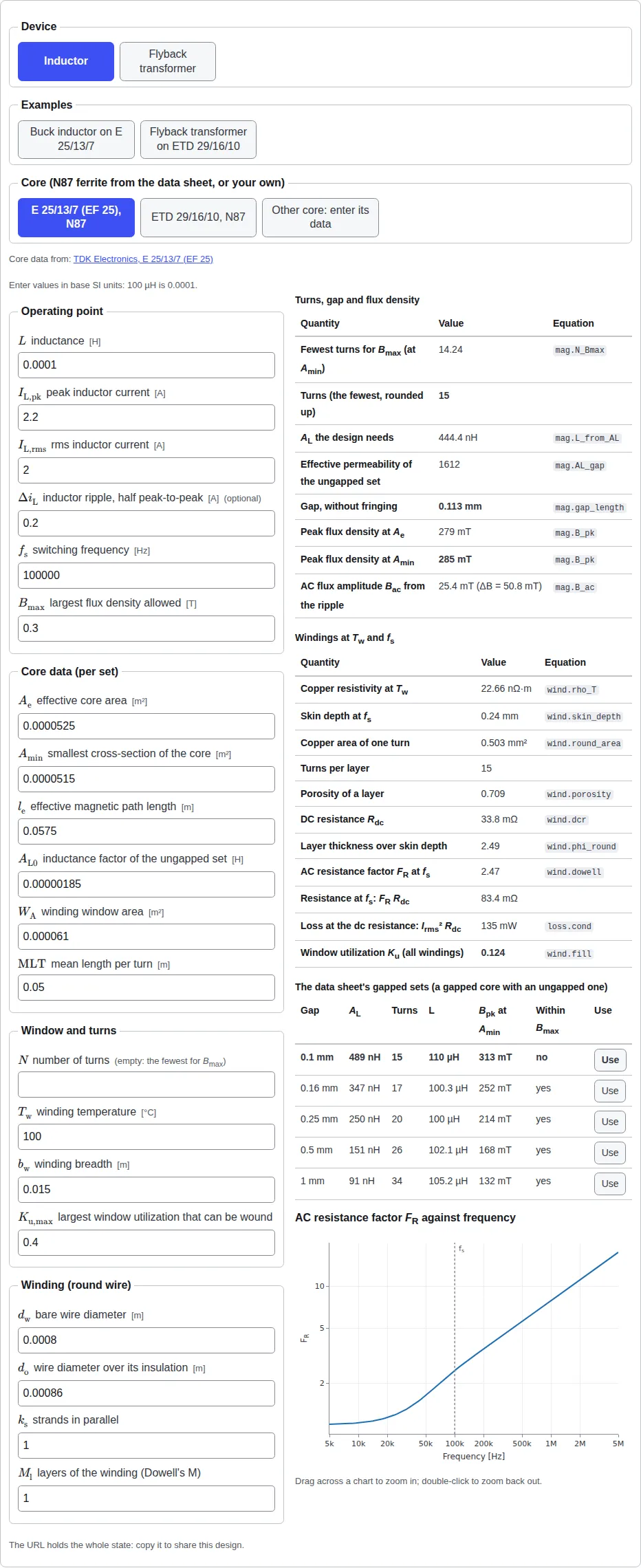
The numbers in the examples, presets and exercises on this site are synthetic: round teaching values, not data from any real design.